Apollo 300
StratusTM P300
StratusTM P500
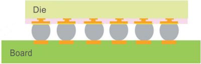
Bumping is an advanced wafer level process technology where “bumps” or “balls” made of various metals are formed on the substrate before the wafer or board is cut, or “diced” into individual chips. Wafer bumping is an essential part of flip chip or board level semiconductor packaging which has become the standard in interconnect technology in consumer electronics today. These “bumps” are the components that connect the die to the substrate and become the package after singulation. These interconnect building blocks can be bumps or copper pillars, composed of metal solders, such as eutectic or lead free SnAg.
The bumps, or pillars, provide shorter pathways than wire bonds between die and substrate to improve the electrical, mechanical and thermal performance of the flip chip package. For the performance driven market, flip chip interconnects reduce signal propagation delay, provide better bandwidths, and relieve the constraints of power distribution. Bump composition and dimension depends on requirements such as final form factor, cost and the electrical, mechanical and thermal performance. Cu Pillar structures have become the interconnect solution of choice for fine pitch, lead-free, or high current application devices. For the form factor driven market, such as mobile applications, replacing wire bonding by flip chip interconnects reduces the size and weight of the package as well as delivering better performance.
 Source: Collection of Advanced Packaging reports Yole Développement, 2018 www.i-micronews.com
Cu Pillar
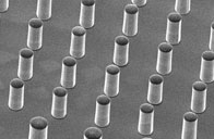
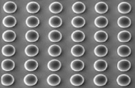
Bumps
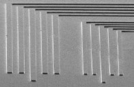
RDL
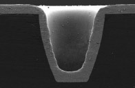
Via Fill
Product Offering
ASMPT NEXX offering sputtering and plating wafer and panel level solution for the bumping process. NEXX offers features and options to support both current processes and variations which evolve as the interconnection market matures. NEXX serves the high volume manufacturing portion of the bumping market.
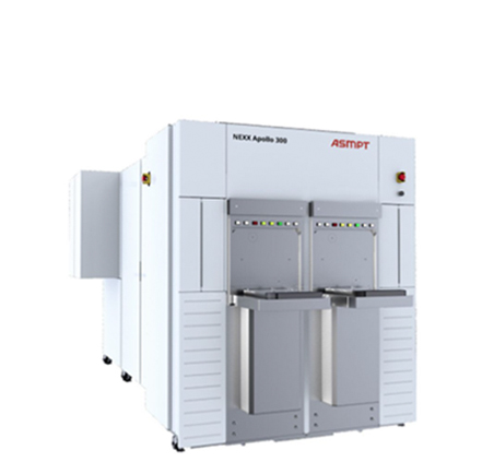
Wafer Sputtering – Apollo 300
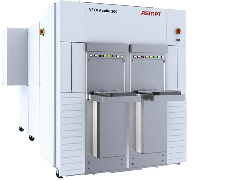
Apollo Under Bump Metallization (UBM) is an in-line physical vapor deposition system for customers who manufacture multiple advanced packaging features, such as a range of copper redistribution layers (RDL), the Apollo UBM produces both thick and thin films in the most compact footprint on the market.
Benefits
- High throughput sputtering solution for thick and thin films
- Stress management to reduce wafer and die warpage
- Handles multiple wafer sizes
- Safer handling of an array of wafer types
- Up to 5 different metals
- Degas
- DC Pulsed Sputtering
- Backside Gas (BSG)
- Reactive Sputtering
- RF Bias
- ICP and CCP etch
- Electrostatic chucks
- Bridge tool capability
- Fully configurable
- Processes 300 and 200 mm wafers
200

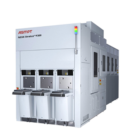
For customers who manufacture multiple advanced packaging features including the standard copper pillar interconnects and microbumps. The P300’s high speed wafer handling system delivers the flexibility and extendibility to produce both large and small features.
- Highest productivity plating tool on the market
- Process RDLs, Copper Pillars and TSVs in one tool
- Handles multiple wafer sizes
- Safer handling of an array of wafer types
- Shields make faster plating possible while maintaining good within wafer uniformity
Features
- Up to 6 different chemistries
- Various reservoir sizes for high or low volume plating Chemistry stabilizing cell technology (SnAg and Ni)
- ShearPlate Technology
- Up to 30 wafer processing
- Bridge tool capability
- Fully configurable
- Processes 300 and 200 mm wafers
Related products: S300, S200
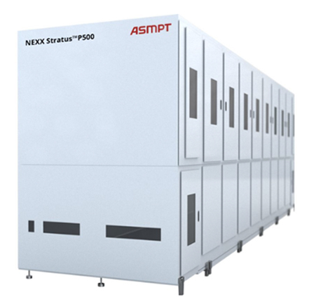
Panel Plating – StratusTM P500

The StratusTM P500 has been proven to deliver wafer scale plating precision on panels up to 510 x 515 mm at the leading panel makers. This panel scale plating tool is a semiconductor industry game changer because it brings higher quality, wafer level chemistries to glass and epoxy panel substrates.
Benefits
- Highest technology panel plating tool on the market delivering <10 um RDL L/S and an array of advanced packaging features
- Safer handling of thin, bowed and warped panels
- Shields make faster plating possible while maintaining good within panel uniformity
Features
- Up to 5 different chemistries
- Various reservoir sizes for high or low volume plating Membrane cell technology
- ShearPlate Technology
- Segmented anodes
- Single or Dual sided plating
- Bridge tool capability
- Fully configurable
- Processes 510 x 515 mm panels